Thursday 31 January 2013

Focused Ion-Beam Machining


                  Focused Ion-Beam Machining
 Focused ion beam, also known as FIB, is a technique used particularly in the semiconductor industry, materials science and increasingly in the biological field for site-specific analysis, deposition, and ablation of materials. An FIB setup is a scientific instrument that resembles a scanning electron microscope (SEM). However, while the SEM uses a focused beam of electrons to image the sample in the chamber, an FIB setup uses a focused beam of ions instead. FIB can also be incorporated in a system with both electron and ion beam columns, allowing the same feature to be investigated using either of the beams. FIB should not be confused with using a beam of focused ions for direct write lithography (such as in proton beam writing). These are generally quite different systems where the material is modified by other mechanisms.
  click here to see video

http://www.ionbeammilling.com/images/milling.gif

Principle

The principle of FIB
Focused ion beam (FIB) systems have been produced commercially for approximately twenty years, primarily for large semiconductor manufacturers. FIB systems operate in a similar fashion to a scanning electron microscope (SEM) except, rather than a beam of electrons and as the name implies, FIB systems use a finely focused beam of ions (usually gallium) that can be operated at low beam currents for imaging or high beam currents for site specific sputtering or milling.

block diagram
As the diagram on the right shows, the gallium (Ga+) primary ion beam hits the sample surface and sputters a small amount of material, which leaves the surface as either secondary ions (i+ or i-) or neutral atoms (n0). The primary beam also produces secondary electrons (e). As the primary beam rasters on the sample surface, the signal from the sputtered ions or secondary electrons is collected to form an image.
At low primary beam currents, very little material is sputtered and modern FIB systems can easily achieve 5 nm imaging resolution (imaging resolution with Ga ions is limited to ~5 nm by sputtering and detector efficiency). At higher primary currents, a great deal of material can be removed by sputtering, allowing precision milling of the specimen down to a sub micrometre or even a nano scale.

Technology

http://upload.wikimedia.org/wikipedia/commons/0/0a/Sch%C3%A9ma_FIB.jpg


Usage

Unlike an electron microscope, FIB is inherently destructive to the specimen. When the high-energy gallium ions strike the sample, they will sputter atoms from the surface. Gallium atoms will also be implanted into the top few nanometers of the surface, and the surface will be made amorphous.
Because of the sputtering capability, the FIB is used as a micro- and nano-machining tool, to modify or machine materials at the micro- and nanoscale. FIB micro machining has become a broad field of its own, but nano machining with FIB is a field that is still developing. Commonly the smallest beam size for imaging is 2.5–6 nm. The smallest milled features are somewhat larger (10–15 nm) as this is dependent on the total beam size and interactions with the sample being milled.


http://www.icss.soton.ac.uk/images/raw/degroot-spin-torque.png

Helium ion microscope (HeIM)

Another ion source seen in commercially available instruments is a helium ion source, which is inherently less damaging to the sample than Ga ions although it will still sputter small amounts of material especially at high magnifications and long scan times. As helium ions can be focused into a small probe size and provide a much smaller sample interaction than high energy (>1 kV) electrons in the SEM, the He ion microscope can generate equal or higher resolution images with good material contrast and a higher depth of focus. Commercial instruments are capable of sub 1 nm resolution.

http://www.asu.edu/clas/csss/NUE/img/Dual-BeamFIB.png

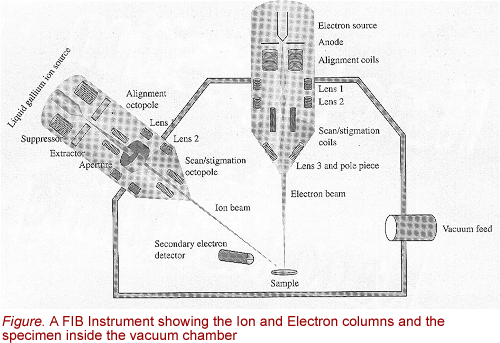
The applications of FIB include :


  • cross-sectional imaging through semiconductor devices (or any layered structure)
  • modification of the electrical routing on semiconductor devices
  • failure analysis
  • preparation for physico-chemical analysis
  • preparation of specimens for transmission electron microscopy (TEM)
  • preparation of samples for AtomProbe analysis
  • micro-machining
  • mask repair
  • non-semiconductor applications


Electron-Beam Machining (EBM)


               Electron beam machining

Electron-beam machining (EBM) is a process where high-velocity electrons concentrated into a narrow beam are directed toward the work piece, creating heat and vaporizing the material. EBM can be used for very accurate cutting or boring of a wide variety of metals. Surface finish is better and kerf width is narrower than those for other thermal cutting processes.
http://electron-beam-machining.beamss.info/images/electron-beam-welding-machine-2.jpg

Process

To achieve the fast evaporation of the material, the power planar density in the beam cross-section must be as high as possible: - values up to 10^7 W/mm^2 can be achieved at the spot of impact. As the electrons transfer their kinetic energy into heat in a very small volume, the material impacted by the beam is evaporated in very short time.

http://electron-beam-machining.beamss.info/images/electron-beam-machining-3.jpg

Equipment

EBM equipment in construction is similar to electron beam welding machines (see electron beam welding). EBM machines usually utilize voltages in the range of 150 to 200 kV to accelerate electrons to about 200,000 km/s. Magnetic lenses are used to focus the electron beam to the surface of the work-piece. By means of electromagnetic deflection system the beam is positioned as needed, usually by means of a computer.
http://www.barc.gov.in/technologies/images/ebwm-2.png

Electron-beam machining (EBM)

The EBM technique is used for cutting fine holes and slots in any material. In a vacuum chamber, a beam of high-velocity electrons is focused on a workpiece. The kinetic energy of the electrons, upon striking the workpiece, changes to heat, which vaporizes minute amounts of the material. The vacuum prevents the electrons from scattering, due to collisions with gas molecules. EBM is used for cutting holes as small as 0.001 inch (0.025 millimetre) in diameter or slots as narrow as 0.001 inch in materials up to 0.250 inch (6.25 millimetres) in thickness. EBM is also used as an alternative to light optics manufacturing methods in the semiconductor industry. Because electrons have a shorter wavelength than light and can be easily focused, electron-beam methods are particularly useful for high-resolution lithography and for the manufacture of complex integrated circuits. Welding can also be done with an electron beam, notably in the manufacture of aircraft engine parts.


Laser-Beam Machining (LBM)


                  Laser beam machining

            Laser Beam machining (LBM) is an unconventional machining process in which a beam of highly coherent light called a Laser is directed towards the work piece for machining. Since the rays of a laser beam are monochromatic and parallel it can be focused to a very small diameter and can produce energy as high as 100 MW of energy for a square millimeter of area. It is especially suited to making accurately placed holes. It can be used to perform precision micro-machining on all microelectronic substrates such as ceramic, silicon, diamond, and graphite. Examples of microelectronic micro-machining include cutting, scribing & drilling all substrates, trimming any hybrid resistors, patterning displays of glass or plastic and trace cutting on semiconductor wafers and chips. A pulsed ruby laser is normally used for developing a high power.


Process description
A coherent beam of monochromatic light is focused on the workpiece causing material removal by vaporisation. Machines are generally CAD/CAM compatible, with 3-axis and 5-axis machines being generally available.
Profile creation of sheet metal parts is the most common applications, but it is also possible to drill holes and create blind features in many different types of material.
Gas-assisted laser beam machining is common. The gas type can be oxygen, inert gas, or air, depending on material type and quality requirements.


http://www.emeraldinsight.com/content_images/fig/0330270307009.png

  Typical Uses


  • Profiling of sheet parts.
  • Holes (0.005mm diameter to 1.3mm), profiling, scribing, engraving and trimming.
  • Prototype parts.
  • Non-standard shaped holes, slots and profiling.
  • Features in silicon wafers (electronics industry).
  • Small diameter lubrication holes.
  • Suitable for thin or delicate parts as there is no mechanical contact.

http://image.thefabricator.com/a/articles/photos/523/fig1a.jpg 


 Design guidelines
  • Lasers work best on materials such as carbon steel or stainless steels. Metals such as aluminium and copper alloys are more difficult to cut due to their ability to reflect the light as well as absorb and conduct heat. This requires lasers that are more powerful.
  • LBM is not a bulk material removal process. It is most suited to contour cutting, slitting and drilling small diameter deep holes (length to diameter ratios of up to 50:1 are possible).
  • There are special methods to create blind or stepped features, but they are less accurate.
  • Sharp corners are possible, but radii should be provided for in the design.
  • Some distortion may be caused in very thin parts.
  • Maximum workpiece thickness: mild steel = 25mm, stainless steel = 13mm, aluminium 10mm.
  • Localised thermal stresses and heat affected zones result.


Process variations


  • LBT (Laser Beam Torch). Uses a simultaneous gas stream
  • Laser Texturing and Laser Etching are performed at lower energy levels.
  • Surface hardening. Laser Beam Welding (LBW).
  • Laser marking or laser printing can be used to create graphics, text or barcodes on most materials.
  • LBM can also be integrated well with sheet metal cutting processes. For example, the Trumpf Laserpress (created in 1979).

The environment

  • The heat may potentially cause the generation of toxic fumes.


The economics

  • Production rates are moderate to high.
  • Higher material removal rate than with conventional machining.
  • High power consumption.
  • Short lead times.
  • Tooling and equipment costs very high. Some skilled labour required.
  • Very fast with high degree of automation possible.
  • Burrs are very small, reducing the need for secondary finishing operations.
  • Considerable economies can be obtained by stacking sheets for simultaneous cutting.


Wednesday 30 January 2013

Electrical Discharge Machining


          Electrical Discharge Machining
                            (EDM)

What is EDM? A Brief History

Xact Wire EDM process
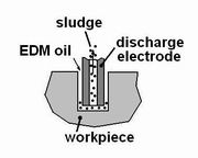
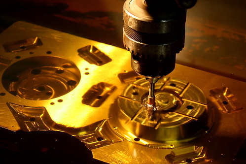
The acronym EDM is derived from Electrical Discharge Machining.
The EDM process we know today started with the observations of Joseph Preistly in 1770. He noticed that electrical discharges had removed material from the electrodes in his experiments. This is also known as electro-discharge erosion.
In the 1940's Soviet researchers developed a machining process that formed the foundation for modern EDM.

Electric Discharge Machining

Xact Wire EDM Spark PropertiesThe basic EDM process is really quite simple. An electrical spark is created between an electrode and a work piece. The spark is visible evidence of the flow of electricity. This electric spark produces intense heat with temperatures reaching 8000 to 12000 degrees Celsius, melting almost anything. The spark is very carefully controlled and localized so that it only affects the surface of the material. The EDM process usually does not affect the heat treat below the surface. With wire EDM the spark always takes place in the dielectric of deionized water. The conductivity of the water is carefully controlled making an excellent environment for the EDM process. The water acts as a coolant and flushes away the eroded metal particles.


http://jetbeetle.com/X150_image/EDM_Drill.JPG

      Types
  1. Sinker EDM

Sinker EDM, also called cavity type EDM or volume EDM, consists of an electrode and workpiece submerged in an insulating liquid such as, more typically, oil or, less frequently, other dielectric fluids. The electrode and workpiece are connected to a suitable power supply. The power supply generates an electrical potential between the two parts. As the electrode approaches the workpiece, dielectric breakdown occurs in the fluid, forming a plasma channel, and a small spark jumps.
These sparks usually strike one at a time because it is very unlikely that different locations in the inter-electrode space have the identical local electrical characteristics which would enable a spark to occur simultaneously in all such locations. These sparks happen in huge numbers at seemingly random locations between the electrode and the workpiece. As the base metal is eroded, and the spark gap subsequently increased, the electrode is lowered automatically by the machine so that the process can continue uninterrupted. Several hundred thousand sparks occur per second, with the actual duty cycle carefully controlled by the setup parameters. These controlling cycles are sometimes known as "on time" and "off time", which are more formally defined in the literature.

Wire EDM

In wire electrical discharge machining (WEDM), also known as wire-cut EDM and wire cutting, a thin single-strand metal wire, usually brass, is fed through the workpiece, submerged in a tank of dielectric fluid, typically deionized water. Wire-cut EDM is typically used to cut plates as thick as 300mm and to make punches, tools, and dies from hard metals that are difficult to machine with other methods.
The wire, which is constantly fed from a spool, is held between upper and lower diamond guides. The guides, usually CNC-controlled, move in the xy plane. On most machines, the upper guide can also move independently in the zuv axis, giving rise to the ability to cut tapered and transitioning shapes (circle on the bottom square at the top for example). The upper guide can control axis movements in xyuvijkl–. This allows the wire-cut EDM to be programmed to cut very intricate and delicate shapes.

Applications

Prototype production

The EDM process is most widely used by the mold-making tool and die industries, but is becoming a common method of making prototype and production parts, especially in the aerospace, automobile and electronics industries in which production quantities are relatively low. In sinker EDM, a graphite, copper tungsten or pure copper electrode is machined into the desired (negative) shape and fed into the workpiece on the end of a vertical ram.

http://www.triz-journal.com/library/graphics/2009-06-vsrs_03.gif

Coinage die making

For the creation of dies for producing jewelry and badges, or blanking and piercing (through use of a pancake die) by the coinage (stamping) process, the positive master may be made from sterling silver, since (with appropriate machine settings) the master is significantly eroded and is used only once. The resultant negative die is then hardened and used in a drop hammer to produce stamped flats from cutout sheet blanks of bronze, silver, or low proof gold alloy. For badges these flats may be further shaped to a curved surface by another die. This type of EDM is usually performed submerged in an oil-based dielectric. The finished object may be further refined by hard (glass) or soft (paint) enameling and/or electroplated with pure gold or nickel. Softer materials such as silver may be hand engraved as a refinement.

Metal disintegration machining

Several manufacturers produce EDM machines for the specific purpose of removing broken tools (drill bits or taps) from work pieces. In this application, the process is termed "metal disintegration machining".

Advantages and disadvantages

Some of the advantages of EDM include machining of:
  • Complex shapes that would otherwise be difficult to produce with conventional cutting tools.
  • Extremely hard material to very close tolerances.
  • Very small work pieces where conventional cutting tools may damage the part from excess cutting tool pressure.
  • There is no direct contact between tool and work piece. Therefore delicate sections and weak materials can be machined without any distortion.
  • A good surface finish can be obtained.
  • Very fine holes can be easily drilled.
Some of the disadvantages of EDM include:
  • The slow rate of material removal.
  • The additional time and cost used for creating electrodes for ram/sinker EDM.
  • Reproducing sharp corners on the workpiece is difficult due to electrode wear.
  • Specific power consumption is very high.
  • Power consumption is high.
  • "Overcut" is formed.
  • Excessive tool wear occurs during machining.
  • Electrically non-conductive materials can be machined only with specific set-up of the process.